0:06
Russia has taken another step towards
0:09
strengthening its domestic semiconductor
0:11
manufacturing capabilities.
0:13
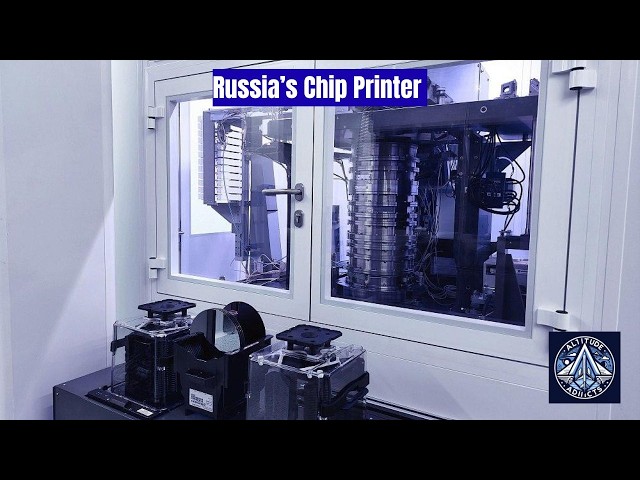
A newly developed photoiththography
0:15
system has now been added to the state
0:17
industrial information system often
0:22
The equipment was created by the
0:24
Zelenograd Nanotechnology Center
0:26
commonly referred to as ZNTC.
0:29
It is used to transfer circuit designs
0:31
onto semiconductor wafers during the
0:34
production of integrated circuits.
0:37
Altitude Addicts, the YouTube channel
0:39
presenting this analysis, explains that
0:42
the system has officially been listed as
0:44
industrial equipment available for use
0:47
within Russia's semiconductor sector.
0:50
Its listing marks an important step in
0:52
building a domestic micro electronics
0:54
manufacturing ecosystem.
0:57
The system is capable of achieving a
0:59
resolution of 350 nanometers.
1:03
This level of precision allows the
1:05
production of very large scale
1:09
The equipment is identified in the
1:10
catalog under the designation RAVC
1:18
Although the name is technical, the
1:20
machine's purpose is straightforward.
1:23
It transfers microscopic circuit
1:25
patterns onto silicon wafers. These
1:28
patterns eventually become the
1:30
transistors and connections inside
1:34
To understand the importance of this
1:36
machine, it helps to look at
1:38
photoiththography itself.
1:41
Photoiththography is the central process
1:43
that makes semiconductor manufacturing
1:47
In this process, ultraviolet light is
1:50
used to project circuit patterns onto a
1:52
photosensitive material deposited on a
1:54
silicon wafer. These patterns are
1:57
created using a template called a photo
2:01
Altitude Addicts explains that after
2:03
exposure, the wafer underos additional
2:08
This processing converts the pattern
2:10
into the blueprint for micro electronic
2:14
The new system developed by ZNTTC uses a
2:17
projection exposure method. Instead of
2:20
placing the mask directly on the wafer,
2:22
the image is projected optically.
2:25
This improves precision and allows
2:28
patterns to be repeated across the wafer
2:31
Each layer of circuitry must also be
2:34
aligned with previous layers.
2:37
Altitude Addicts notes that alignment
2:39
accuracy is extremely important in
2:41
semiconductor fabrication.
2:44
Even tiny errors can ruin an entire
2:47
According to the catalog description,
2:49
the system supports the production of
2:51
circuits with a design rule of 0.35
2:57
This equals 350 nanome.
3:00
Although this is not the most advanced
3:02
semiconductor technology, it is still
3:05
widely used. Many industrial and
3:08
automotive chips are produced using
3:10
similar process nodes.
3:12
Altitude addicts explains that such
3:14
technologies are common in power
3:16
electronics, embedded systems, and
3:19
industrial controllers.
3:21
These applications prioritize
3:23
reliability rather than extreme
3:27
The system was developed and
3:28
manufactured in Russia.
3:31
However, the official catalog entry
3:33
notes that this classification is based
3:35
on the manufacturer's declaration.
3:39
Independent verification of the full
3:41
level of domestic production has not
3:43
been publicly confirmed.
3:45
Nevertheless, the development represents
3:47
a significant step for Russian
3:50
semiconductor equipment.
3:52
Altitude Addicts explains that the
3:54
Zelenograd Nanotechnology Center plays a
3:57
key role in Russia's micro electronics
4:01
The organization develops semiconductor
4:03
technologies and advanced manufacturing
4:07
It is located in the city of Zelenograd
4:11
This region is often described as the
4:13
country's equivalent of Silicon Valley.
4:17
The lithography system was reportedly
4:19
introduced into production during the
4:24
This means it is a relatively recent
4:26
addition to Russia's semiconductor
4:28
technology portfolio.
4:30
The equipment is designed to process
4:32
wafers with a diameter of up to 200 mm.
4:36
This wafer size remains widely used
4:39
across many semiconductor factories.
4:42
Altitude Addicts notes that 200 mm
4:45
wafers are commonly used to produce
4:47
microcontrollers, sensors, and power
4:51
They are especially common in mature
4:53
semiconductor manufacturing processes.
4:56
Resolution is one of the most important
4:59
parameters for lithography equipment. It
5:02
determines the smallest features that
5:04
can be printed on a wafer.
5:07
In this case, the machine can produce
5:09
structures about 350 nanome wide. That
5:14
is roughly 1/3 of a micrometer.
5:17
The system operates using ultraviolet
5:19
light with a wavelength of approximately
5:25
This wavelength is associated with what
5:27
is known as ey line lithography.
5:31
Altitude Addicts explains that modern
5:33
cuttingedge semiconductor factories
5:35
often use shorter wavelengths.
5:38
These include deep ultraviolet and
5:40
extreme ultraviolet technologies.
5:43
However, lithography remains useful for
5:46
mature semiconductor processes.
5:49
Many industrial chips do not require the
5:51
smallest possible transistor sizes.
5:55
Another important parameter is alignment
5:59
Each layer of a semiconductor chip must
6:01
align precisely with the previous
6:03
layers. According to reports, the system
6:06
achieves alignment accuracy of
6:08
approximately 90 nanome.
6:11
This level of precision helps prevent
6:13
manufacturing defects.
6:16
Altitude addicts notes that the working
6:18
exposure field measures about 22x 22 mm.
6:23
Chip patterns can be repeated across the
6:25
wafer through a step and repeat process.
6:29
The development of the system involved
6:32
international cooperation.
6:34
ZNTTC worked together with the
6:36
Bellarusian company Planner.
6:39
Development reportedly began in the year
6:44
It was completed several years later
6:46
with support from Russia's Ministry of
6:51
Altitude Addicts explains that Bellarus
6:53
has long experience in semiconductor
6:55
production equipment.
6:58
Several companies there originated from
7:00
the Soviet micro electronics industry.
7:03
Although 350 nanometer technology may
7:06
sound outdated, it remains extremely
7:08
useful. Many modern devices still rely
7:12
on these manufacturing nodes.
7:15
Power management chips, industrial
7:17
sensors, and automotive electronics
7:19
often use processes between 180 and 500
7:24
These technologies emphasize durability
7:29
Altitude Addicts explains that aerospace
7:31
electronics and telecommunications
7:33
infrastructure also rely on such
7:37
Radiation tolerance and reliability are
7:40
more important than maximum transistor
7:44
Developing domestic lithography tools is
7:46
therefore strategically important. It
7:49
allows Russia to continue producing
7:51
essential electronics.
7:54
Photoiththography machines are among the
7:56
most complex devices used in
7:58
semiconductor manufacturing.
8:00
Only a few companies globally produce
8:03
the most advanced systems.
8:06
Altitude Addicts notes that major global
8:08
manufacturers include ASML, Nikon, and
8:10
Canon. Their machines require extremely
8:14
advanced optical and engineering
8:18
Even building equipment for mature
8:20
semiconductor nodes represents a
8:22
significant technical achievement.
8:24
Domestic production reduces reliance on
8:29
The listing of the new system in the
8:31
state industrial information system also
8:34
has practical importance.
8:36
The platform acts as a national catalog
8:39
of industrial technologies. Government
8:42
agencies and state companies often
8:45
consult this catalog when purchasing
8:48
This helps domestically develop
8:50
technology reach industrial customers.
8:54
Altitude Addicts explains that the
8:56
catalog also supports import
8:58
substitution policies.
9:00
Domestic equipment gains priority in
9:02
publicly funded projects.
9:05
Although the current system operates at
9:07
350 nanometers, development work
9:12
Future versions are expected to reach
9:14
resolutions around 130 nanome.
9:18
Such improvements would allow the
9:19
production of more advanced circuits.
9:23
These nodes were widely used by global
9:25
semiconductor manufacturers in the early
9:29
Altitude Addicts explains that advancing
9:32
lithography technology is extremely
9:36
Progress requires improvements in
9:37
optics, vibration isolation, and
9:42
Precision wafer handling and
9:44
environmental control are also
9:46
essential. All components must operate
9:49
with extraordinary accuracy.
9:52
The Zelenograd Nanotechnology Center
9:54
operates in the city that remains the
9:56
heart of Russia's micro electronics
10:00
Zelenograd was originally created during
10:02
the Soviet era as a center for
10:05
semiconductor development.
10:07
Today, the region hosts research
10:09
institutes, chip manufacturers, and
10:11
technology companies. Together, they
10:14
form the backbone of Russia's
10:16
semiconductor ecosystem.
10:18
Altitude Addicts concludes that the new
10:21
photoiththography system represents
10:23
another step toward a self-sufficient
10:25
semiconductor industry. Although the
10:28
technology is not the most advanced
10:30
globally, it remains crucial for many
10:33
industrial applications.
10:35
By developing domestic manufacturing
10:38
equipment, Russia aims to secure the
10:40
production of chips for sectors such as
10:42
energy, transportation,
10:44
telecommunications, and defense.
10:47
Future improvements in lithography
10:49
technology could further expand these
10:55
If you like the video, please subscribe,
10:57
share, and like. Also, please take the
11:00
membership of Altitude Addicts to