0:06
At a seminar held at the Institute of
0:08
Semiconductor Physics of the Siberian
0:10
branch of the Russian Academy of
0:12
Sciences in Novo Subursk, candidate of
0:14
physical and mathematical sciences,
0:17
Dimmitri Sheg discussed the potential
0:20
development of X-ray lithography
0:22
technology in Russia through the use of
0:24
the new skiff facility which is
0:26
currently undergoing commissioning in
0:30
According to him, Skype could play a
0:32
crucial role in creating a fundamentally
0:35
new platform for microlithography based
0:37
on the X-ray spectrum, thereby helping
0:40
to overcome existing technological
0:42
limitations in electronics.
0:45
The skiff experiment is only one element
0:47
within a broader scientific landscape.
0:50
It represents mega science level
0:52
infrastructure forming a cuttingedge
0:55
foundation for research in physics,
0:57
material science, biology and other
1:01
The facility has entered the
1:02
commissioning phase near Nova Suburk
1:05
with initial scientific experiments
1:07
scheduled to begin in 2025.
1:11
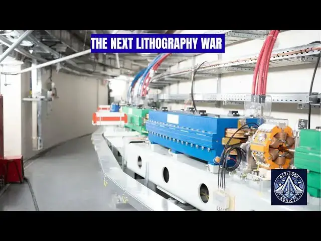
The Siberian circular photon source
1:13
known as KE is an advanced fourth
1:16
generation synretron radiation facility
1:18
with an electron energy of 3 giga
1:21
electron volts. It is being constructed
1:24
in the nova suburk region as a major
1:26
national scientific installation
1:28
combining accelerator systems with
1:31
experimental stations that allow
1:32
researchers to work with highly
1:34
brilliant intense and coherent x-ray
1:39
A defining scientific characteristic of
1:41
skiff is its ultra low emittance, a
1:44
parameter describing the purity and
1:46
focusability of the electron beam. Low
1:49
emittance enables extremely high
1:51
brightness, strong coherence, and a
1:53
narrow angular spread of radiation.
1:56
These properties are essential for the
1:58
most demanding experiments in both
2:00
fundamental and applied science.
2:03
The facility is being developed within
2:05
Russia's national project titled science
2:08
and universities with the participation
2:10
of the Budker Institute of Nuclear
2:13
Physics of the Siberian branch of the
2:15
Russian Academy of Sciences and other
2:18
research organizations.
2:20
The complex will include multiple
2:22
experimental beam lines, engineering
2:24
systems, laboratories, and support
2:26
infrastructure dedicated to solving
2:28
problems ranging from material science
2:31
and chemistry to biology and
2:35
Synretron radiation is electromagnetic
2:38
emission produced when charged
2:39
particles, primarily electrons, are
2:42
accelerated within magnetic fields. This
2:45
radiation possesses unique qualities
2:47
including extremely high brightness, a
2:50
broad spectral range extending from
2:52
infrared to hard X-rays, strong
2:54
directionality and coherence, and
2:56
precise spectral tunability.
2:59
These characteristics make synretron
3:01
radiation an indispensable tool for
3:04
atomic scale structural analysis.
3:07
It enables research spanning from
3:09
biomolelecular crystalallography to the
3:11
study of ultraast phenomena in advanced
3:15
Today more than 50 synretron radiation
3:18
facilities operate worldwide as major
3:21
national and international research
3:22
centers. These include ERF in France,
3:26
MAX 4 in Sweden, Diamond Light Source in
3:28
the United Kingdom and NSLS2 in the
3:31
United States. Together they provide
3:34
millions of research hours to scientists
3:36
working in material science, energy,
3:38
chemistry, biology, and medicine.
3:42
Lithography is the foundational
3:44
technology used to fabricate circuit
3:46
patterns on semiconductor substrates.
3:49
It defines the geometry and dimensions
3:51
of micro electronic components directly
3:54
influencing performance, energy
3:56
efficiency, and functional capability of
3:58
modern electronic devices.
4:01
The prevailing global standard in
4:03
semiconductor manufacturing relies on
4:05
extreme ultraviolet lithography which
4:08
operates at a wavelength of
4:10
approximately 13.5 nanome.
4:13
This technology supports the production
4:15
of advanced chips at companies such as
4:17
TSMC, Samsung, and Intel. Further
4:21
miniaturization, however, requires even
4:23
shorter wavelengths, making X-ray
4:25
lithography a potential next step.
4:29
So far, large-scale industrial adoption
4:32
of X-ray lithography has been limited by
4:34
substantial technical challenges.
4:37
These include the need for ultrarecise
4:39
radiation sources, advanced optical
4:41
systems, highly accurate photo masks,
4:43
X-ray sensitive resists, specialized
4:46
instrumentation, and extremely stable
4:48
vacuum environments. If these barriers
4:51
are overcome, X-ray lithography could
4:54
enable dramatic feature scaling and
4:56
entirely new semiconductor
5:00
According to Dimmitri Shegll and other
5:02
Russian researchers, SKF's unique
5:04
properties make it a promising platform
5:07
for X-ray lithography experiments.
5:10
As a bright and highly coherent X-ray
5:12
source, skiff can be adapted for complex
5:15
studies involving the formation of micro
5:17
and nanoructures using X-ray radiation.
5:21
This approach represents a direct link
5:23
between fundamental science and applied
5:27
Using a synretron source, scientists can
5:30
test new photomask materials, study
5:32
exposure regimes, analyze interactions
5:35
between X-rays and resists, and develop
5:37
experimental techniques that could later
5:39
form the basis of industrial X-ray
5:44
As a result, she emphasized researchers
5:47
are gaining an exceptionally powerful
5:49
tool. He urged active participation and
5:52
stressed the importance of securing beam
5:54
lines in the next construction phase for
5:57
semiconductor and solid state physics
6:01
At present, no large-scale commercial
6:03
semiconductor factories use synretron
6:06
radiation directly for mass production
6:10
The global industry continues to rely
6:12
primarily on extreme ultraviolet
6:14
scanners produced by ASML.
6:17
Nevertheless, research into X-ray
6:19
lithography is ongoing.
6:21
For example, a United States startup
6:23
named Substrate has introduced an X-ray
6:26
lithography system based on particle
6:29
accelerators that could potentially
6:30
achieve critical dimensions of around 2
6:35
This positions it as a possible
6:36
alternative or complement to extreme
6:39
ultraviolet technology.
6:41
In addition, many synretron facilities
6:44
worldwide already use X-ray beams for
6:46
deep X-ray lithography, also known as
6:51
Facilities such as Anka in Germany have
6:53
demonstrated the effectiveness of
6:55
synretronbased X-ray lithography for
6:58
producing extremely precise
7:00
microructures even though it is not yet
7:02
used for mainstream semiconductor
7:06
There is also growing interest in X-ray
7:08
free electron lasers which generate
7:10
ultrashort and highly intense X-ray
7:14
These sources may become critical for
7:16
future lithography methods and for
7:18
studying ultraast structural changes in
7:23
For SKF to function as a practical
7:25
platform for advancing X-ray
7:27
lithography, several major challenges
7:29
must be addressed. These include the
7:32
development of advanced X-ray optics for
7:34
beam shaping and focusing, creation of
7:37
stable and sensitive X-ray resists,
7:39
improvements to synchronization and
7:41
control systems, and achieving long-term
7:44
stability suitable for industrial use.
7:47
Many of these issues remain research
7:49
topics rather than fully engineered
7:53
However, the existence of a powerful
7:56
domestic synretron facility provides the
7:58
conditions necessary for systematic
8:01
experimentation and for attracting
8:03
collaborative research efforts.
8:06
The skiff project in Akadam Gordoc
8:08
represents far more than a new
8:10
scientific installation.
8:12
It forms a cornerstone for a new phase
8:15
of technological development in Russia.
8:18
By combining fundamental research with
8:20
applied potential, skiff opens
8:22
opportunities in X-ray lithography, a
8:25
key technology for the future of micro
8:28
If Russia successfully leverages SCF's
8:31
capabilities and builds a strong
8:33
ecosystem of scientists, engineers, and
8:36
technologists around it, the facility
8:38
could provide a significant competitive
8:40
advantage on the global stage. It would
8:43
support progress in material science and
8:46
highresolution structural analysis and
8:48
may ultimately enable breakthroughs in
8:51
semiconductor manufacturing.
8:54
At a time when micro electronics
8:56
development is increasingly constrained
8:58
by the physical limits of existing
9:00
lithographic methods, infrastructure
9:03
projects like SCF may serve as catalysts
9:06
for redefining how future microchips are
9:08
designed and produced from foundational
9:11
experiments to transformative industrial
9:17
If you like the video, please subscribe,
9:20
share and like. Also, please take the
9:22
memberships to encourage us.