0:05
What if I told you that Russia is
0:07
pouring billions into a secret weapon
0:09
for tech independence, and it isn't what
0:14
Forget about lithography machines for a
0:15
second. Today, we are breaking down two
0:18
massive high-stakes microelectronics
0:20
projects that Moscow just green-lit. We
0:23
will look at the secret tech called
0:25
epitaxy, how they plan to clone Western
0:27
machines, and the astronomical tech
0:31
Watch till the end to see how this
0:33
reshapes the global semiconductor
0:37
Russia has furthered its long-term quest
0:39
to reestablish critical semiconductor
0:41
manufacturing capabilities by starting
0:44
two significant microelectronics
0:46
projects that are designed to strengthen
0:49
domestic epitaxy equipment.
0:52
Epitaxy is a manufacturing process that
0:54
deposits a thin crystalline layer onto a
0:57
crystalline base in an organized manner.
1:00
The new layer is forced to grow in the
1:01
exact same crystal structure and
1:04
orientation as the underlying substrate,
1:07
which functions as a seed crystal.
1:10
In early June 2026, the Russian Ministry
1:13
of Industry and Trade published
1:15
procurement documents that indicated
1:17
nearly 2 billion rubles had been
1:19
allocated to the development of two
1:21
advanced categories of semiconductor
1:23
manufacturing systems.
1:26
These systems are presently dominated by
1:31
Now, what is the big deal with epitaxy
1:34
As mentioned, it is a technologically
1:36
challenging stage of chip production
1:38
that involves the growth of ultra-thin
1:40
crystalline semiconductor layers on
1:43
silicon or compound semiconductor
1:46
These layers form the foundation of many
1:48
modern electronic, photonic, and radio
1:53
Epitaxial growth is essential for for
1:55
high-performance transistors, power
1:57
electronics, microwave components, laser
2:00
devices, and advanced sensors.
2:03
Following years of sanctions and export
2:05
restrictions that have limited access to
2:07
Western technology, Moscow's initiative
2:10
is indicative of its overarching
2:12
strategy to decrease its reliance on
2:15
imported semiconductor equipment.
2:18
Look, let's be real for a second.
2:20
Building these complex machines from
2:22
scratch is an absolute beast of a task.
2:25
But the Russian government has
2:27
partitioned the effort into two distinct
2:29
programs to make it happen.
2:32
The first and more significant
2:33
undertaking is designated as Citadel and
2:36
has a budget of approximately 1.5
2:41
It concentrates on the creation of a
2:43
molecular beam epitaxy system that is
2:45
capable of fabricating sophisticated
2:48
compound semiconductor heterostructures.
2:51
These heterostructures are composed of
2:52
materials such as gallium arsenide,
2:57
compounds, and aluminum gallium
2:58
semiconductor structures.
3:01
The second project, epitaxy SiGe, has
3:04
been allocated approximately 463.7
3:08
million rubles and is designed to
3:10
develop a chemical vapor phase epitaxy
3:12
system for silicon and silicon germanium
3:15
semiconductor layers on 200 mm
3:19
In recent years, Russia has made one of
3:21
its most extensive efforts to localize
3:23
sophisticated semiconductor
3:25
manufacturing equipment, as opposed to
3:28
relying on imported tools to produce
3:31
Collectively, the programs represent
3:35
If we shift our focus to why this
3:37
matters, we see that although
3:39
lithography machines are often the
3:40
subject of public debate regarding
3:42
semiconductors, epitaxy systems are
3:45
similarly important for many electronic
3:50
Epitaxy enables manufacturers to
3:52
cultivate crystalline layers that are
3:54
exceedingly pure and possess electrical
3:56
properties that are methodically
3:58
managed. The process allows engineers to
4:01
build structures that would be
4:02
unfeasible to produce using conventional
4:04
bulk semiconductor materials alone.
4:07
Modern telecommunications devices,
4:09
military radar systems, satellite
4:12
electronics, photonics devices, and
4:14
high-speed processors all depend on
4:16
epitaxially grown layers.
4:19
Epitaxial layers increase the
4:21
reliability and efficacy of transistors
4:25
Epitaxy facilitates the production of
4:28
optoelectronic components and
4:30
high-frequency components that are used
4:32
in defense and communications
4:34
applications for compound semiconductors
4:36
like gallium arsenide.
4:39
Only a small number of companies
4:40
worldwide manufacture epitaxy equipment,
4:43
which needs ultra-high vacuum systems,
4:45
precise temperature control,
4:47
sophisticated robotics, and advanced
4:52
This brings us directly to the Citadel
4:54
molecular beam epitaxy system itself.
4:57
The Citadel project, which is more
4:59
comprehensive, aims to develop a
5:01
molecular beam epitaxy platform that is
5:04
domestic and can replace foreign systems
5:07
like the American Veeco Gen 200 and the
5:10
French Riber 49. Currently, there are no
5:14
direct industrial Russian equivalents in
5:16
this category of equipment as indicated
5:18
by Russian procurement documentation.
5:21
Let's zoom out and look at how crazy
5:23
precise this technology actually is.
5:27
Molecular beam epitaxy is one of the
5:29
most precision semiconductor
5:31
manufacturing technologies currently
5:34
The wafer surface is targeted by beams
5:37
of atoms, which are deposited one atomic
5:39
layer at a time under ultra-high vacuum
5:43
This enables engineers to generate
5:45
semiconductor structures that are
5:47
exceedingly complex with remarkable
5:49
control over their composition and
5:53
It is expected that the upcoming Russian
5:55
system will facilitate the bulk
5:57
processing of multiple wafers
6:01
The apparatus must be able to
6:02
accommodate a minimum of 5 76 mm
6:06
substrates or 3 100 mm substrates in a
6:09
single processing cycle as required by
6:12
the design specifications.
6:14
This capability is crucial because it
6:16
boosts productivity and reduces
6:18
manufacturing expenses in comparison to
6:21
systems that process wafers
6:25
Looking closely at the fine print, the
6:27
tender documentation's stringent
6:29
technical specifications emerge as one
6:32
of the most noteworthy features of the
6:35
The molecular beam epitaxy chamber must
6:38
attain a residual pressure that is
6:40
extremely low, measured in fractions of
6:42
a trillionth of atmospheric pressure
6:46
It is important to preserve these vacuum
6:48
levels as even microscopic contamination
6:51
can modify the electrical properties of
6:53
semiconductor layers.
6:56
The wafer surface must also be subjected
6:58
to highly uniform deposition by the
7:02
Thickness variation targets are limited
7:04
to a mere few percent and pharmaceutical
7:07
uniformity requirements are equally
7:11
Furthermore, the machine is expected to
7:13
integrate 10 molecular beam source ports
7:15
with sophisticated analytical systems
7:17
and large crucible volumes.
7:20
The following are included: infrared
7:22
optical pyrometry for real-time process
7:25
monitoring and reflection high-energy
7:27
electron diffraction diagnostics.
7:30
According to Altitude Addicts tracking
7:32
global supply chains, these
7:34
characteristics are typically associated
7:37
with advanced industrial semiconductor
7:39
fabrication systems and research systems
7:42
that are used by major international
7:46
This leads right into the details of the
7:48
Epitaxy SiGe project. The second
7:51
initiative is directed at a specific
7:53
industry of semiconductor manufacturing.
7:56
The Epitaxy CE program will concentrate
7:59
on the development of equipment for
8:01
silicon and silicon germanium epitaxial
8:04
growth on 200 mm wafers, rather than
8:07
compound semiconductors.
8:10
Silicon germanium technology is widely
8:12
used in specialized integrated circuits,
8:15
data communications hardware, radio
8:17
frequency electronics, and
8:18
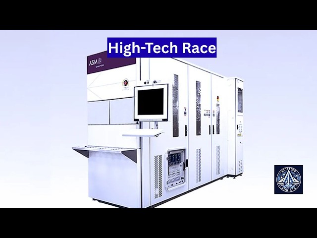
high-performance transistors. The system
8:21
is designed to serve as a domestic
8:22
alternative to the Epsilon 2000
8:25
platform, which is manufactured by ASM
8:30
The undertaking necessitates the
8:32
creation of three critical subsystems.
8:35
A robotic wafer handling system, a dry
8:38
chemical wafer cleansing module, and a
8:40
deposition reactor that facilitates
8:42
epitaxial growth are all included in the
8:45
Its purpose is to prepare substrates for
8:49
Hey, if you are still trying to
8:51
visualize how intense this environment
8:55
While operating within a broad pressure
8:57
range, the reactor faces temperatures
9:04
To reach the requisite crystal quality
9:06
for the precision growth of silicon and
9:08
silicon germanium layers, these
9:10
conditions are essential.
9:13
Additionally, Russian planners have
9:15
specified performance objectives, which
9:17
include silicon growth rates of at least
9:22
Beyond just assembling the parts, the
9:24
program's emphasis on domestic content
9:27
is perhaps its most noteworthy feature.
9:30
The Ministry of Industry and Trade is
9:32
not just seeking a Russian branded
9:34
version that is assembled from imported
9:38
The procurement documents explicitly
9:40
stipulate that critical subsystems, such
9:42
as vacuum chambers, compressors,
9:44
molecular beam sources, vacuum valves,
9:47
and control systems must be of Russian
9:50
origin whenever feasible.
9:52
Formal justification and ministry
9:54
sanction are required for the use of
9:57
imported alternatives, which are only
9:59
permissible in exceptional
10:02
This requirement is indicative of a more
10:05
extensive trend in Russia's industrial
10:08
Russian authorities have been
10:10
concentrating on technological
10:11
sovereignty since 2022
10:14
to mitigate the vulnerabilities that are
10:17
a result of their dependence on foreign
10:19
suppliers for strategic technologies.
10:22
Industry. Altitude Addicts note that
10:25
semiconductor manufacturing equipment
10:27
faces significant challenges due to
10:30
reliance on a limited number of
10:31
international suppliers for specialized
10:33
components like vacuum gauges,
10:35
controllers, power supplies, and
10:37
precision motion systems.
10:40
This highlights the immense challenges
10:44
The development of competitive
10:46
semiconductor equipment remains an
10:48
extraordinarily complex effort despite
10:50
considerable funding by Russian
10:54
Veeco, Riiber, and ASM International
10:57
have worked for decades to refine their
10:59
technologies and develop a wealth of
11:01
engineering expertise.
11:03
Advanced material science, vacuum
11:06
engineering, automation, software
11:08
development, thermal management, and
11:10
process control technologies are all
11:12
integrated into modern epitaxy systems.
11:16
In addition to hardware development, the
11:18
domestic replication of these
11:19
capabilities will necessitate the
11:21
establishment of specialized engineering
11:23
talent and manufacturing supply chains.
11:27
Certification is an additional obstacle.
11:30
Before implementing new equipment for
11:32
production, semiconductor manufacturers
11:35
typically necessitate years of testing.
11:38
Even if Russian developers are able to
11:40
build functional systems, their
11:42
pervasive industrial adoption will be
11:45
contingent upon their ability to
11:46
demonstrate economic viability,
11:48
repeatability, and reliability.
11:52
When we look at the long-term timelines,
11:54
the true scale of the operation becomes
11:58
The magnitude of the project is
11:59
exemplified by the Ministry of Industry
12:02
and Trade's established timelines.
12:05
The Epitaxy C project is expected to be
12:07
finalized by June 2029.
12:10
It is expected that the Citadel
12:12
molecular beam epitaxy system, which is
12:14
more ambitious, will continue until
12:19
These extended schedules suggest that
12:21
the government regards the initiative as
12:23
a long-term strategic investment, rather
12:26
than a short-term industrial
12:30
These two epitaxy programs are part of a
12:32
broader Russian initiative to
12:34
rehabilitate the domestic semiconductor
12:38
Moscow has initiated initiatives that
12:40
concentrate on semiconductor materials,
12:42
chip design software, electronic
12:44
components, manufacturing equipment, and
12:47
packaging technologies in recent years.
12:51
The development of domestic epitaxy
12:53
equipment addresses a significant gap in
12:55
the country's technology ecosystem,
12:57
despite the fact that Russia continues
13:00
to lag behind global leaders in advanced
13:02
semiconductor manufacturing.
13:05
Russia could acquire local access to
13:07
equipment required for the production of
13:09
silicon germanium devices, gallium
13:12
arsenide components, microwave
13:14
electronics, photonic systems, and other
13:16
specialized semiconductor products that
13:19
are crucial for both civilian and
13:21
defense industries if the projects
13:23
achieve their technical objectives.
13:26
Market Altitude Addicts closely watching
13:28
this space point out that it remains to
13:30
be resolved whether these systems will
13:32
ultimately achieve performance levels
13:34
that are comparable to those of
13:36
established Western platforms.
13:40
Nevertheless, the extensive funding, the
13:42
rigorous technical specifications, and
13:45
the emphasis on domestic subsystems
13:47
suggest that Russia is making a
13:48
concerted effort to consolidate its
13:51
influence over one of the most critical
13:53
sectors of semiconductor manufacturing
14:00
We thank the people who have subscribed
14:02
the channel, liked, and shared the
14:05
We also thank the channel members for
14:09
Last but not least, we also thank the
14:11
viewers who have hyped our videos.