0:06
One of the most strategically critical
0:07
sectors of the 21st century is the
0:10
global semiconductor industry.
0:13
Microelectronics are essential to nearly
0:16
every aspect of contemporary existence
0:19
from defense systems and advanced
0:20
computing to artificial intelligence and
0:25
In this context, Russia has accelerated
0:28
its efforts to achieve technological
0:30
self-reliance by attempting to modernize
0:32
and reconstruct its domestic
0:34
semiconductor ecosystem.
0:37
The Zelenograd Nanotechnology Center,
0:39
often called ZNTC, is right at the
0:41
center of this transformation.
0:44
It's evolving quickly, bringing together
0:46
research, engineering, and actual
0:48
production into one connected platform.
0:51
The story really becomes clearer when
0:54
you look at the momentum.
0:56
Recent developments at ZNTC include new
0:58
facilities, improvements in chip
1:00
packaging, and steady progress in
1:04
All of this points toward something
1:06
bigger, a full-cycle microelectronics
1:08
industry slowly taking shape inside
1:12
Microelectronics is no longer just
1:14
another industrial sector.
1:17
It now directly influences national
1:19
security, economic resilience, and
1:21
technological competitiveness.
1:24
For years, Russia depended heavily on
1:26
imported semiconductor technologies,
1:28
especially advanced manufacturing tools
1:33
That dependence created weak points,
1:35
particularly in high-tech industries
1:37
where reliability and independence
1:41
ZNTC's mission is built around fixing
1:44
The center is working across the entire
1:46
semiconductor chain, from design to
1:49
packaging to testing, to build domestic
1:53
The goal isn't instant parity with
1:57
It's something more realistic and
1:58
long-term. A system that can sustain
2:03
And honestly, that kind of foundation
2:05
matters more than flashy short-term
2:09
Back in April 2026, insights into this
2:12
direction came through an interview with
2:16
He outlined not just current projects,
2:19
but the broader ambition.
2:21
ZNTC, according to him, isn't only
2:23
scaling production, it's preparing for
2:26
the next generation of microelectronics
2:30
Under his leadership, the center has
2:32
taken on a dual role.
2:34
It acts as both a technological
2:36
innovator and an industrial enabler.
2:39
Work spans advanced packaging,
2:41
lithography systems, and newer ideas
2:43
like chiplet-based architectures.
2:46
It's a bit like building both the tools
2:48
and the factory at the same time.
2:52
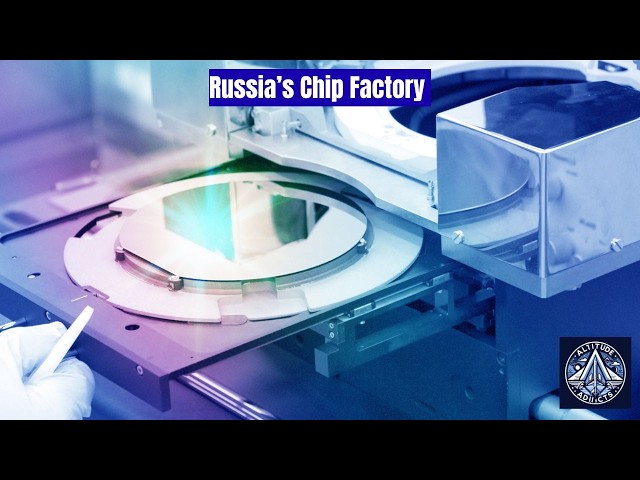
One of the most visible signs of
2:53
progress came in January 2026.
2:57
That's when a new 1,200 square meter
3:00
assembly and testing facility was
3:04
This marked a serious upgrade in
3:06
Russia's ability to process and package
3:08
semiconductor components domestically.
3:12
The facility can handle up to 200,000
3:14
microchips per month.
3:17
It supports both large industrial orders
3:19
and small specialized production runs.
3:23
That flexibility is important because
3:25
the market ranges from mass consumer
3:27
electronics to very niche defense or
3:32
The real strength of the facility lies
3:34
in advanced packaging formats like PBGA,
3:39
These are essential for modern
3:40
high-performance chips.
3:43
They allow better heat management,
3:44
tighter integration, and improved
3:46
electrical performance.
3:49
In simple terms, they make chips more
3:51
powerful and more reliable.
3:54
And here's something practical.
3:56
The facility was built with scaling in
4:00
With further investment, production
4:02
could rise to 500,000 packages per
4:06
So, it's not just about today, it's
4:08
clearly built for future demand.
4:11
The journey to this point didn't happen
4:15
Back in 2021, ZNTC mastered
4:18
three-dimensional assembly technology.
4:21
Then in 2023, it developed its first
4:23
domestic multiplexer.
4:26
Step by step, capability has been
4:30
By 2026, the launch of advanced BGA
4:33
packaging lines marked another leap.
4:35
These systems allow more complex
4:37
circuits to fit into smaller spaces.
4:41
It's a quiet kind of progress, but
4:45
The facility supports die sizes from 5
4:48
by 5 mm up to 25 by 25 mm.
4:52
Lead pitch can go down to .8 mm with
4:56
even finer options being explored.
4:59
That kind of range makes it adaptable
5:03
There's also a strong focus on thermal
5:07
Especially for power and microwave
5:09
electronics, managing heat is critical.
5:12
ZNTC is working on specialized
5:14
enclosures and materials to handle this.
5:18
Because overheating, well, it ruins
5:21
Lithography, of course, remains one of
5:24
the toughest challenges.
5:26
In 2025, ZNTC began selling its first
5:29
domestic lithography systems at 350
5:34
Not cutting-edge globally, but still a
5:36
major milestone locally.
5:39
The next step is already planned.
5:42
A 130 nanometer facility is targeted for
5:47
That shift alone could significantly
5:49
improve chip performance and efficiency.
5:53
At the same time, work is ongoing on
5:55
electron beam lithography at 150
6:00
This is more precise and suited for
6:02
specialized applications.
6:04
It's not mass production, but it's
6:06
important for pushing boundaries.
6:09
Another key development is defect
6:13
Systems are being built to detect
6:14
irregularities as small as 45
6:19
That level of precision is crucial for
6:21
maintaining quality and yield.
6:24
ZNTC is also developing photolithography
6:27
cluster systems for deep ultraviolet
6:30
These will support very large-scale
6:32
integrated circuits on 200 mm wafers.
6:36
It's a move toward more industrial-scale
6:40
And this is where things get
6:43
Chiplet technology is now under
6:45
development in collaboration with NIIMA
6:49
The idea is to combine five separate
6:51
chips on a single silicon interposer.
6:55
Instead of one big chip, you get
6:57
multiple smaller ones working together.
7:00
It's more flexible, often cheaper, and
7:04
Globally, this is becoming a major
7:06
trend, and ZNTC is stepping into it
7:10
Quality control is another area where
7:12
the center is focusing heavily.
7:15
The assembly line achieves yields of
7:19
That's supported by detailed inspection
7:24
Most materials used in production are
7:26
domestically sourced.
7:28
Some specialized chemicals still come
7:30
from abroad, especially photoresists.
7:33
But there are active efforts to replace
7:35
those with local alternatives.
7:39
Collaboration is also key.
7:41
ZNTC works with companies like Baikal
7:43
Electronics and MCST.
7:46
These partnerships help build a broader
7:50
This is something Altitude Addicts has
7:52
been tracking closely.
7:54
Not just the technology, but how the
7:56
ecosystem is forming around it.
7:59
Of course, challenges remain.
8:02
The global semiconductor industry is
8:04
dominated by a few very advanced
8:08
Catching up isn't easy, and it won't
8:12
Access to advanced equipment and skilled
8:14
personnel is still limited.
8:17
But progress is steady.
8:19
Maybe slower than headlines suggest, but
8:23
The road map is clear.
8:25
Better packaging, improved lithography,
8:28
and expansion into new technologies like
8:31
It's all building toward something
8:35
And yes, Altitude Addicts has covered
8:37
similar transitions before. This one
8:39
just feels more layered.
8:42
In the end, the development of ZNTC
8:45
reflects a broader shift in Russia's
8:47
technological direction.
8:49
It's about rebuilding capability step by
8:53
The new facility, producing hundreds of
8:55
thousands of chips monthly, is a major
8:59
Combined with research and partnerships,
9:01
it shows long-term intent.
9:04
Altitude Addicts sees this as more than
9:08
It's about reshaping how a country
9:10
approaches microelectronics entirely.
9:14
And while challenges remain, the
9:18
ZNTC isn't standing still, it's moving
9:20
forward one layer at a time.
9:25
If you like the video, please subscribe,
9:28
share, and like. Also, please take the
9:30
membership of the channel to encourage