0:04
In December 2025, Russia announced the
0:08
development of its first entirely
0:10
domestically produced equipment for
0:12
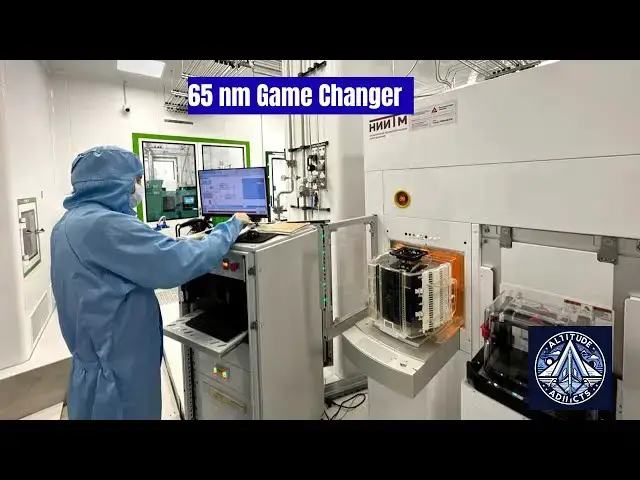
manufacturing integrated circuits. These
0:15
are cluster systems for plasma chemical
0:17
etching and plasma chemical deposition
0:20
designed by Russian research institutes
0:22
on behalf of the Ministry of Industry
0:24
and Trade. The systems support
0:27
technological standards down to 65
0:30
nanome and can process silicon wafers
0:32
with a diameter of up to 300 mm, opening
0:36
new opportunities for modern
0:38
semiconductor production within the
0:42
Plasma chemical etching and plasma
0:44
chemical deposition are core processes
0:46
used in semiconductor fabrication to
0:49
shape and build microscopic structures
0:51
inside a microprocessor.
0:54
In plasma chemical etching, a gas is
0:57
ionized inside a vacuum chamber to
0:59
create plasma and the reactive ions
1:01
precisely remove material from the wafer
1:04
surface at the nanometer scale. This
1:06
allows engineers to form intricate
1:08
patterns such as transistor gates,
1:10
channels, and interconnect pathways.
1:13
Plasma chemical deposition operates in
1:16
the opposite way because it adds
1:18
material rather than removing it.
1:21
plasma activates and deposits extremely
1:23
thin and uniform layers such as silicon
1:25
oxide or silicon nitride onto the wafer.
1:29
These layers function as insulators,
1:32
protective barriers, or structural
1:34
elements within the semiconductor.
1:37
Because both processes occur in a
1:39
controlled environment, they prevent
1:41
contamination and allow manufacturers to
1:43
create highly precise nanocale features
1:46
essential for modern integrated
1:49
The creation of this equipment marks an
1:51
important step toward technological
1:54
independence in micro electronics.
1:56
It greatly strengthens the capabilities
1:58
of Russian manufacturers and reduces
2:01
dependence on foreign suppliers of
2:03
advanced industrial machines.
2:06
The initiative to develop domestic
2:08
semiconductor manufacturing equipment
2:11
emerged as part of the government's
2:12
broader strategy to improve industrial
2:15
self-sufficiency and decrease reliance
2:17
on imported technologies.
2:20
For many years, Russia's micro
2:22
electronics sector lacked specialized
2:24
equipment needed to produce integrated
2:26
circuits with tiny feature sizes. Much
2:29
of the work was done using foreign
2:31
systems creating bottlenecks and
2:34
potential security risks.
2:36
The research institutes NIME, the
2:39
Scientific Research Institute of
2:41
Molecular Electronics and NIITM, the
2:44
Scientific Research Institute of
2:46
Precision Engineering, both part of the
2:48
element group, served as the primary
2:50
developers. The project was carried out
2:53
under a government directive from the
2:56
Ministry of Industry and Trade
2:58
highlighting its national significance.
3:01
The project included designing the
3:03
equipment, constructing clean rooms,
3:05
installing and integrating prototype
3:07
systems, developing technological
3:10
processes, and conducting testing
3:14
Each phase required meticulous precision
3:16
and advanced engineering because the
3:18
apparatus must ensure flawless wafer
3:22
The newly produced systems are
3:25
classified as cluster tools, meaning
3:27
they integrate multiple technological
3:29
modules with a centralized loading
3:31
mechanism. Their main advantage is the
3:34
ability to conduct several sequential
3:37
operations without exposing wafers to
3:39
the atmosphere, which maintains purity
3:41
and improves final product quality.
3:45
A major technological feature of the
3:47
Russian systems is their vacuum-based
3:49
processing method. Wafers remain in a
3:53
vacuum environment for the entire
3:54
duration of processing, never coming
3:57
into contact with air.
3:59
This significantly reduces contamination
4:02
and increases yield. The systems can
4:05
perform essential processes on wafers
4:07
with diameters of 200 mm and 300 mm
4:10
including the deposition of thin
4:12
insulating films such as silicon oxide
4:15
and silicon nitride as well as plasma
4:18
chemical removal used to form
4:22
Plasma etching and plasma deposition
4:24
together make up nearly 1/ half of all
4:27
stages in a semiconductor manufacturing
4:30
cycle. They are essential for creating
4:33
structures, removing materials, and
4:35
forming protective layers.
4:38
The introduction of domestic equipment
4:40
will help Russia modernize its micro
4:43
electronic sector and move closer to
4:45
building a self-reliant technological
4:47
ecosystem. Until now, most high
4:51
precision semiconductor equipment was
4:53
imported, creating strategic risks and
4:55
limiting domestic manufacturers.
4:58
Deputy Minister of Industry and Trade
5:00
Vasilbach stated that the 65 nanometer
5:03
cluster systems meet Russia's long-term
5:06
semiconductor requirements.
5:09
He also emphasized the importance of
5:11
their modular design which increases
5:13
flexibility for different production
5:15
tasks and allows companies to transition
5:18
to more advanced technological nodes in
5:20
the future. Another benefit is that the
5:24
new systems can be used not only in new
5:26
production lines but also in existing
5:28
facilities operating with 200 mm wafer
5:34
This compatibility lets manufacturers
5:36
upgrade capabilities without completely
5:39
rebuilding their plants.
5:41
The development of indigenous cluster
5:43
systems for plasma deposition and
5:45
etching places Russia among a small
5:48
group of nations capable of producing
5:50
such precise equipment.
5:53
Reports state that Russian developers
5:55
now rank among the top five globally in
5:59
In semiconductor manufacturing
6:01
worldwide, cluster systems are
6:03
considered industry standard because
6:05
they combine multiple processes within a
6:08
single vacuum environment, improving
6:10
precision, reducing material waste, and
6:13
boosting overall quality.
6:15
However, reaching the 65 nanometer level
6:18
is only one stage in a long
6:20
technological journey. Leading global
6:23
manufacturers already produce chips with
6:26
features smaller than 10 nanome.
6:29
Achieving such tiny dimensions requires
6:31
further research, greater investment,
6:34
and advanced infrastructure.
6:36
Even so, the 65 nanometer milestone is
6:39
highly important for Russia because
6:41
chips at this scale are used in
6:43
industrial machinery, automobiles,
6:45
automation systems, defense electronics,
6:48
and many other fields.
6:50
Despite the progress, Russia continues
6:53
to face several technological
6:56
Creating domestic photoiththography
6:58
systems, especially for features below
7:01
65 nanometers, remains extremely
7:03
difficult. Current Russian lithography
7:06
tools reportedly have resolutions of
7:08
about 350 nanome, which is far behind
7:12
global leaders using deep ultraviolet
7:15
and extreme ultraviolet technologies.
7:18
In addition, several government programs
7:20
meant to support micro electronics
7:23
struggle with insufficient funding. In
7:26
2025, real spending fell significantly
7:28
below planned levels, potentially
7:31
delaying some future projects.
7:33
Nevertheless, the creation of domestic
7:36
cluster systems is a major technological
7:38
achievement that strengthens Russia's
7:40
scientific and industrial foundation and
7:43
reduces reliance on foreign equipment.
7:47
Developers have already announced plans
7:49
to continue moving forward. After
7:52
completing equipment for the 65
7:54
nanometer node, work is reportedly
7:56
underway on systems that will support
7:58
smaller feature sizes such as 28 nanome
8:02
and below. These nodes are essential for
8:06
high performance processors,
8:07
smartphones, computers, and artificial
8:10
intelligence hardware. Progress in
8:13
related technologies such as
8:15
lithography, thermal treatment, ion
8:17
implantation, and other key
8:19
semiconductor steps will help Russia
8:21
strengthen its capabilities and
8:23
eventually build a complete
8:25
semiconductor production ecosystem.
8:28
With global demand for electronic
8:29
components increasing and micro
8:32
electronics growing in strategic
8:34
importance, the development of domestic
8:36
manufacturing equipment has become a top
8:41
The creation of Russian-made cluster
8:43
systems encourages collaboration among
8:45
industries, boosts engineering
8:47
expertise, and supports scientific
8:51
The development of Russia's first
8:52
cluster systems for plasma chemical
8:55
deposition and etching is a major
8:57
milestone for the nation's scientific
8:59
and industrial progress.
9:02
It demonstrates that Russia can design
9:04
and produce equipment previously
9:06
manufactured only by leading
9:08
international companies.
9:10
Although many challenges remain, this
9:13
achievement strengthens Russia's
9:15
position in the global technological
9:17
arena and lays the groundwork for future
9:19
innovation and development.
9:24
If you think the video was informative,
9:26
please like, subscribe and share. Please
9:29
also take membership of the channel to