0:06
In March 2026, Russia took an important
0:10
step in advanced semiconductor
0:14
Applications opened for its first
0:15
contract-based production of phatonic
0:17
integrated circuits using a multi-RO
0:22
Altitude Addicts, the YouTube channel
0:24
presenting this analysis, explains that
0:27
this marks a major milestone.
0:29
It reflects Russia's push to build a
0:32
domestic futonics ecosystem.
0:34
The initiative is led by Bombman Moscow
0:37
State Technical University in
0:38
partnership with VNIA.
0:41
Together they are creating a shared
0:43
platform for chip design and
0:47
This platform allows startups,
0:49
researchers and companies to build
0:51
photonic chips. Importantly, they do not
0:55
need their own fabrication facilities.
0:58
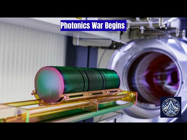
To understand why this matters, we can
1:00
look at the core technology behind the
1:02
project. It is based on silicon nitride
1:08
Altitude addicts explains that silicon
1:10
nitride is known for extremely low
1:12
optical loss. This allows light to
1:16
travel efficiently within chips.
1:18
This property is essential for
1:20
applications like optical communication
1:24
It also supports quantum technologies.
1:27
The process achieves very precise
1:31
The minimum feature size is 70 nanome.
1:35
The minimum spacing is 200 nanome.
1:39
The waveguide thickness is 220 nanome.
1:43
Altitude addicts notes that these
1:45
parameters enable compact and efficient
1:47
photonic devices. They are suitable for
1:51
both research and industry.
1:54
One of the most notable aspects of the
1:56
program is accessibility.
1:58
The pilot run is fully funded for
2:00
Russian scientific teams.
2:03
Participants can receive fabricated
2:05
chips without paying manufacturing
2:09
This lowers the barrier to entry.
2:12
Each participant can receive up to 100
2:14
chip units. These are based on custom
2:19
Altitude Addicts explains that this
2:21
encourages experimentation.
2:23
More ideas can be tested in real
2:27
This initiative uses the multi-RO wafer
2:30
model. This is a well-known concept in
2:32
semiconductor manufacturing.
2:35
Multiple designs from different users
2:38
are combined on a single wafer. After
2:41
fabrication, each user receives their
2:45
This approach reduces costs
2:48
Expenses are shared among participants.
2:52
Altitude Addicts notes that this model
2:54
has been widely used globally.
2:57
It supports innovation in fatonics.
3:00
By introducing this system domestically,
3:02
Russia reduces reliance on foreign
3:06
It strengthens local capabilities.
3:09
The platform also provides a design
3:11
library of standard components.
3:14
These include waveguides, couplers, and
3:18
These components simplify the design
3:20
process. They allow complex circuits to
3:23
be built more easily.
3:26
Altitude Addicts explains that the
3:28
system supports operation at 1550 nanome
3:33
This is important for fiber optic
3:37
Thermoptic modulators are also included.
3:41
They operate at frequencies above 10
3:44
Each chip also includes test structures.
3:48
These allow accurate performance
3:52
Altitude addicts notes that users
3:54
receive detailed measurement data. This
3:57
helps evaluate designs
3:59
beyond fabrication. The program offers
4:02
full support. This includes design,
4:05
modeling, and packaging.
4:07
The Quantum Park team at Bowman
4:09
University provides this assistance.
4:12
It covers the entire development cycle.
4:16
This support is especially useful for
4:19
It simplifies complex processes.
4:23
Altitude Addicts explains that some
4:25
projects may even reach full system
4:28
This speeds up commercialization.
4:32
This initiative is part of a larger
4:34
national program. It falls under the
4:36
priority 2030 framework.
4:40
The goal is to combine different
4:42
computing technologies.
4:44
These include classical, quantum, and
4:48
Phetonic chips play a key role in this
4:50
vision. They use light instead of
4:55
Altitude addicts highlights their
4:59
They offer higher speed and lower energy
5:02
They also generate less heat. This is
5:05
critical for future computing.
5:08
The applications of this technology are
5:11
wide ranging. They extend across many
5:15
These include telecommunications,
5:17
quantum computing, and sensing. They
5:20
also include LAR and medical
5:24
Altitude addicts notes that photonic
5:27
chips are highly versatile.
5:29
They are becoming foundational
5:32
This initiative also improves global
5:36
It positions Russia in the futonic
5:40
By offering domestic fabrication,
5:42
innovation can grow locally. Dependence
5:45
on foreign systems is reduced.
5:48
Altitude Addicts explains that demand
5:50
for phutonics is rising. This is driven
5:54
by artificial intelligence and data
5:58
As demand grows, such platforms become
6:00
more important. They enable faster
6:05
In conclusion, the launch of this
6:07
program marks a new phase in
6:09
technological development. It combines
6:12
advanced materials and accessible
6:16
Altitude Addicts concludes that Phutonix
6:18
represents the future of computing and
6:23
This initiative is a major step toward
6:29
If you like the video, please subscribe,
6:31
share, and like. Also, please take the
6:34
membership of Altitude Addicts to